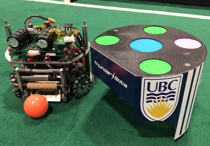
UBC Thunderbots Robot
UBC Thunderbots is an engineering student design team that designs and creates competitive robots to compete in the Small Size League of the international Robocup Federation. In 2019 we were the champions of the Robocup World Cup Competition in Sidney, Australia. In 2020 we are redesigned the entire robot to add new features and be more optimized. As I led the mechanical subteam I also helped design the chipper and kicker components of the new fleet of robots.
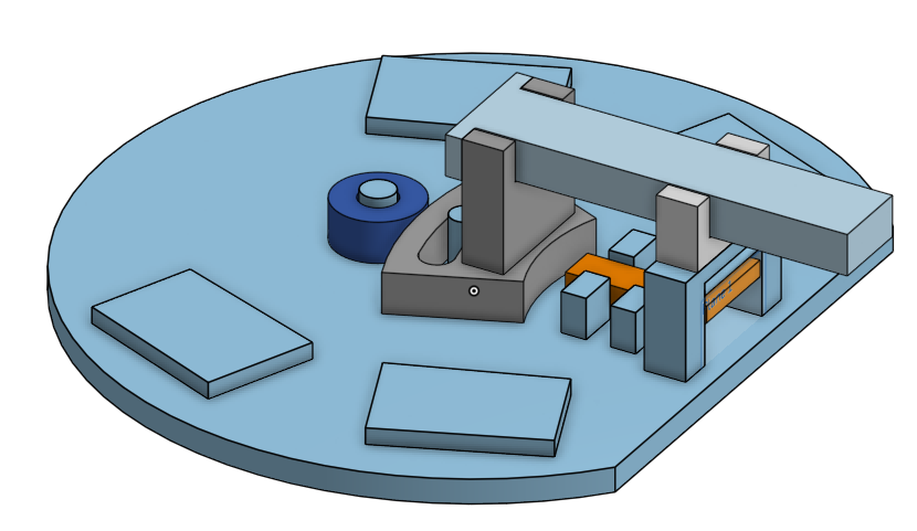
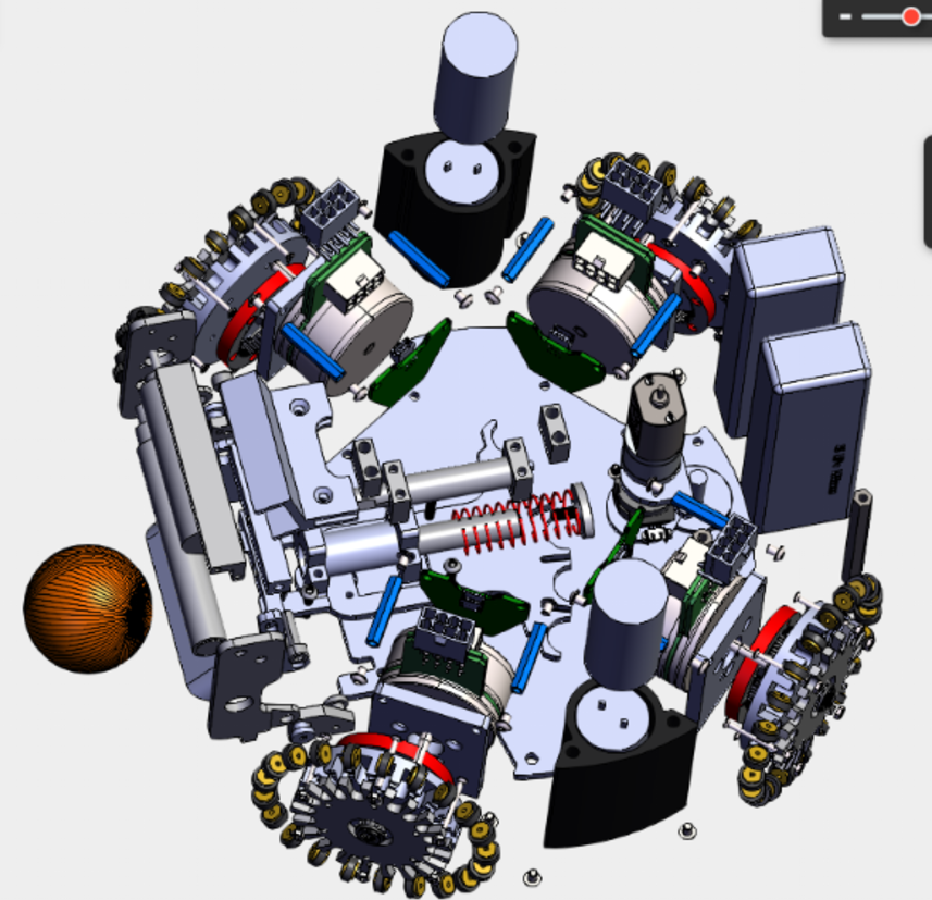
I made this simplified prototype for the kicker and chipper layout for the Thunderbot’s soccer playing robot. The kicker is mounted on a Geneva drive for multiple shooting angles and the chipper is mounted below. This prototype was to generate ideas for saving space.
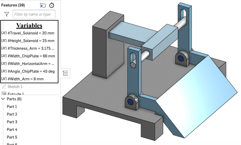
This is a more specific prototype I made of a chipper mechanism based off of what was learned from the above prototype. This one was animated to understand the mechanics and relative dimensions of the movement. I also wrote a MATLAB script that takes the inputs of the dimensions of the chipper and the force from the solenoid, and calculated the output force the chipper makes on the ball. The design and script are to be used together to determine a specific design for the chipper.
MATLAB Code
function [forces] = ChipSimpTransfer(density,soltravel,thickness,armwidth,platewidth,Blength,F,H,angle)
	%%Purpose: Input parameters and Force and output Force of Chip
	% Input:    density: density of material
	%           soltravel: horizontal distance of travel through solenoid
	%           thickness: thickness of arms
	%           armwidth: width of arms
	%           platewidth: width of chipper plate
	%           Blength: length of horizontal arm of chipper
	%           F: Input Force from solenoid
	%           H: Height of center of solenoid from pinned point
	%           angle: angle of chip plate from the ground (45° probably)
	%Output:    [forceoutGp forceoutGs; forceoutJp forceoutJs]
	%               forceoutGp: force at point G assuming thin plate approximation for MMOI
	%               forceoutGs: force at point G assuming slender rod approximation for MMOI
	%               forceoutJp: force at point J assuming thin plate approximation for MMOI
	%               forceoutJs: force at point J assuming slender rod approximation for MMOI
	%%Component Variable Setup
	%Unit conversions for ease of input
	theta=angle*pi/180;
	soltravel=soltravel/1000;a
	thickness=thickness/1000;
	armwidth=armwidth/1000;
	platewidth=platewidth/1000;
	Blength=Blength/1000;
	H=H/1000;
	%Constraints for C
	dimA=[(sqrt(soltravel^2+H^2)+armwidth) armwidth thickness];
	dimB=[(Blength) armwidth thickness];
	dimC=[((0.013+armwidth/2)/sin(theta)) (dimB(2)) (platewidth)];
	%Calculate Masses of each section of the chipper
	ma= density*dimA(1)*dimA(2)*dimA(3);
	mb= density*dimB(1)*dimB(2)*dimB(3);
	mc= density*dimC(1)*dimC(2)*dimC(3);

	%%MMOI Calculations
	%MMOI if Thin Plate Approx
	Iap= 2*(1/12)*ma*(dimA(1)^2+dimA(2)^2)+ma*(dimA(1)^2/4);
	Ibp= 2*(1/12)*mb*((dimB(1)+armwidth)^2+dimB(2)^2)+mb*(dimB(1)^2/4);
	Icp= mc*((1/12)*dimC(1)^2+(dimB(1)+dimC(1)*cos(theta))^2+(dimC(1)*sin(theta))^2); %ThinPlate
	%MMOI if Slender Rod Approx
	Ias= 2*ma*(1/3)*dimA(1)^2;
	Ibs= 2*ma*(1/3)*(dimB(1)+armwidth)^2;
	Ics= mc*((1/12)*dimC(1)^2+(dimB(1)+dimC(1)*cos(theta))^2+(dimC(1)*sin(theta))^2);
	%MMOI about pinned point O
	Iop=Iap+Ibp+Icp; %Thin Plate
	Ios=Ias+Ibs+Ics; %Slender Rod

	%%Angular Acceleration of Chipper
	alphap=(F*H)/(Iop);%Thin Plate
	alphas=(F*H)/(Ios);%Slender Rod

	%%Acceleration of J and G
	%J is point halfway down bar C at 45∫
	%G is point at bottom point of bar C at 45∫
	aGp= alphap*[dimC(1)*sin(theta);dimB(1)+dimC(1)*cos(theta)]; %Thin Plate
	aGs= alphas*[dimC(1)*sin(theta);dimB(1)+dimC(1)*cos(theta)]; %Slender Rod
	aJp= alphap*[dimC(1)/2*sin(theta);dimB(1)+dimC(1)/2*cos(theta)]; %Thin Plate
	aJs= alphas*[dimC(1)/2*sin(theta);dimB(1)+dimC(1)/2*cos(theta)]; %Slender Rod

	%%Force Calculation at chip location
	disp('forces=');
	disp('forceoutGp forceoutGs');
	disp('forceoutJp forceoutJs');
	forces=[norm(aGp)*(ma+mb+mc) norm(aGs)*(ma+mb+mc); norm(aJp)*(ma+mb+mc) norm(aJs)*(ma+mb+mc)];
	% forceoutGp=norm(aGp)*(ma+mb+mc);
	% forceoutGs=norm(aGs)*(ma+mb+mc);
	% forceoutJp=norm(aJp)*(ma+mb+mc);
	% forceoutJs=norm(aJs)*(ma+mb+mc);
As part of the responsibilities as the Mechanical Subteam lead I divided the redesign into subcomponents and distrubted them to teammembers, recruited and mentored new members, investigated better tools for design, led desgin reviews, focused on design for manufacturing, and organized part purchasing.
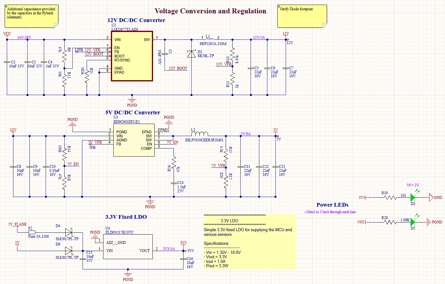
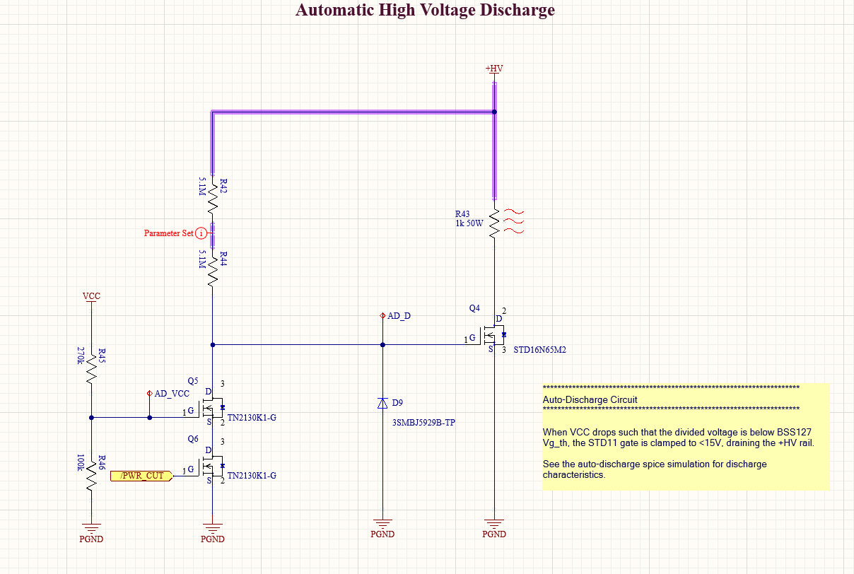
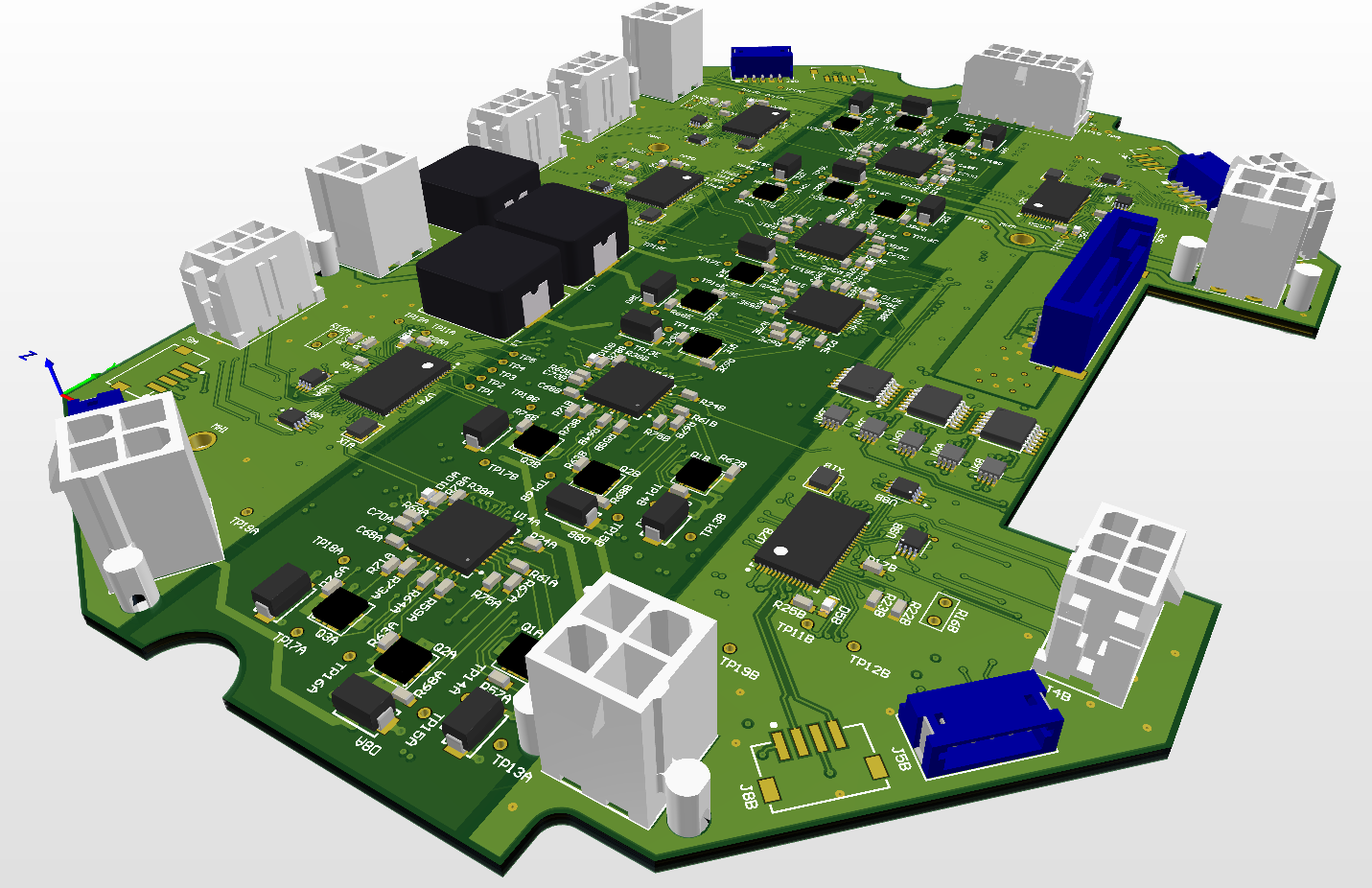
After being mechanical subteam lead for 2 years I decided to transition to an Electrical subteam member to learn more about the electrical design and bringup of the boards necessary for the robot. As part of the electrical subteam I helped design portions of the power board in Altium that converted the battery voltage level down to the various power needs of the chipper/kicker, main MCU board (eventually a Jetson Nano), and motor driver boards.
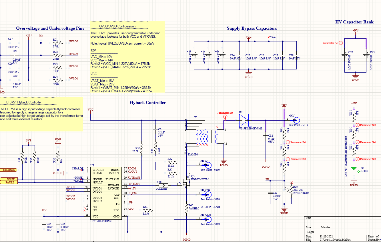
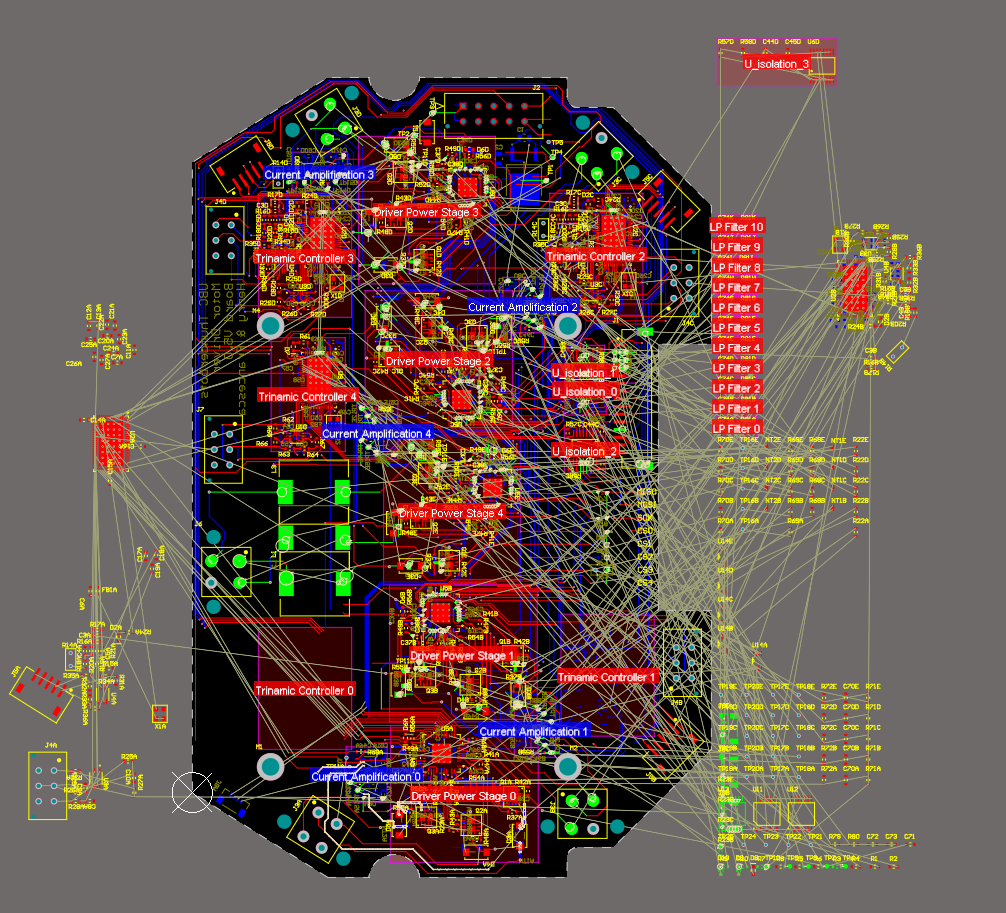
I also mostly helped with the PCB layout of the power board and the more complicated motor driver board shown to the right. Laying out the PCBs taught me to be attentive of manufacturing constraints and also to consider the current expected through different areas of the circuit and to properly give the correct widht trace. Additionally preventing the isolating of ground planes, isolating communication traces as much as posisble, and using a sufficient number of testpoints were all considerations when making the PCBs.
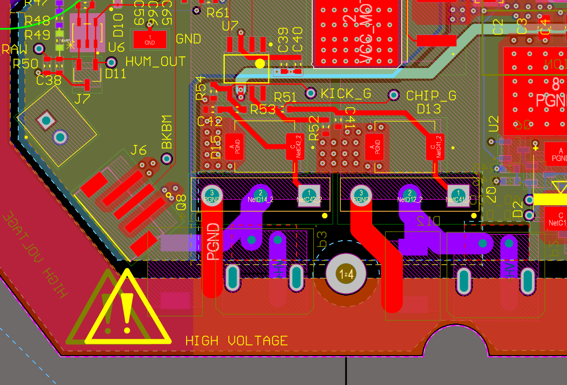
The motor driver board was so complicated it ended up being a six layer PCB with outer component layers, two communication/trace layers, a ground plane, and a power plane.
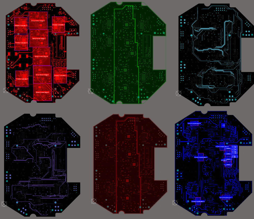
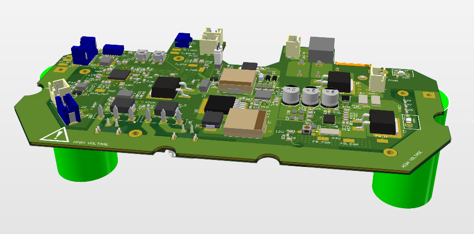
Shown below are the 3D renders of the power board (see left) and motor driver board (see right)
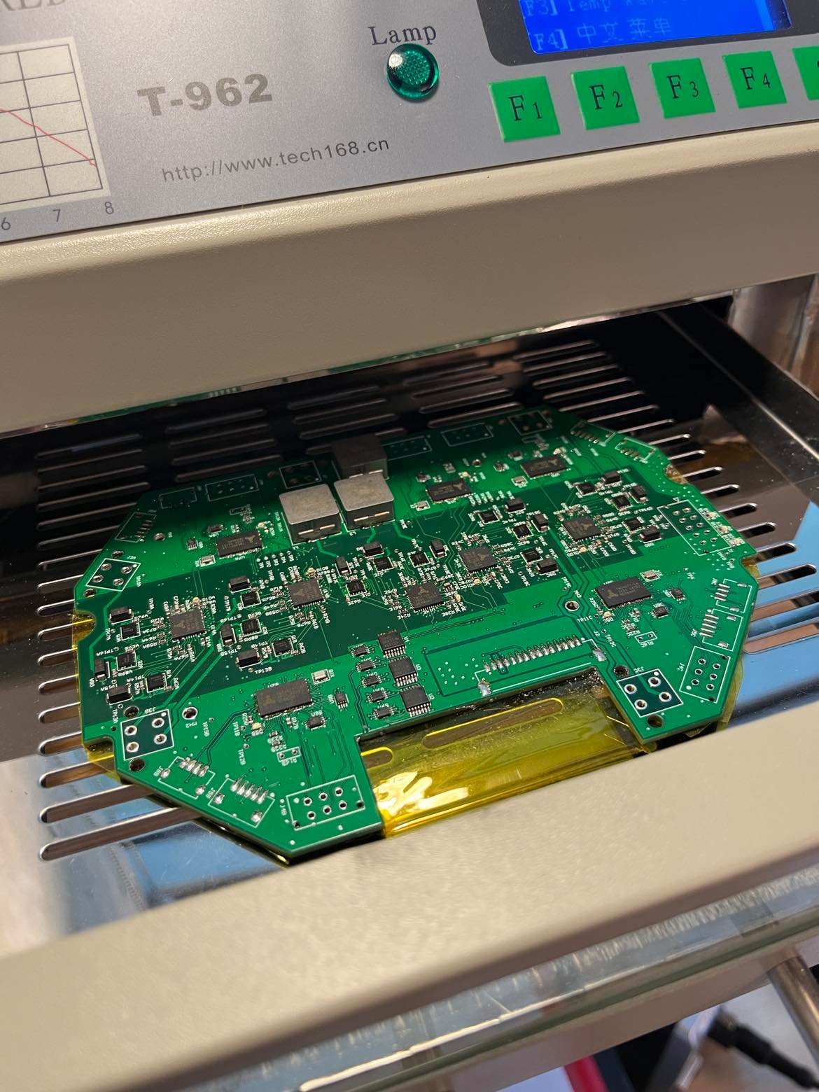
A major part of building the robots that are ready for competition is building, testing, and debugging the various systems of the robot. As a member of the electrical team this involved populating the board with soldering, checking for shorts, writing test scripts to test the solenoid charging and HV sense resistor, testing the regulator outputs, and monitoring the regulator outputs after high current events such as kicking or chipping.
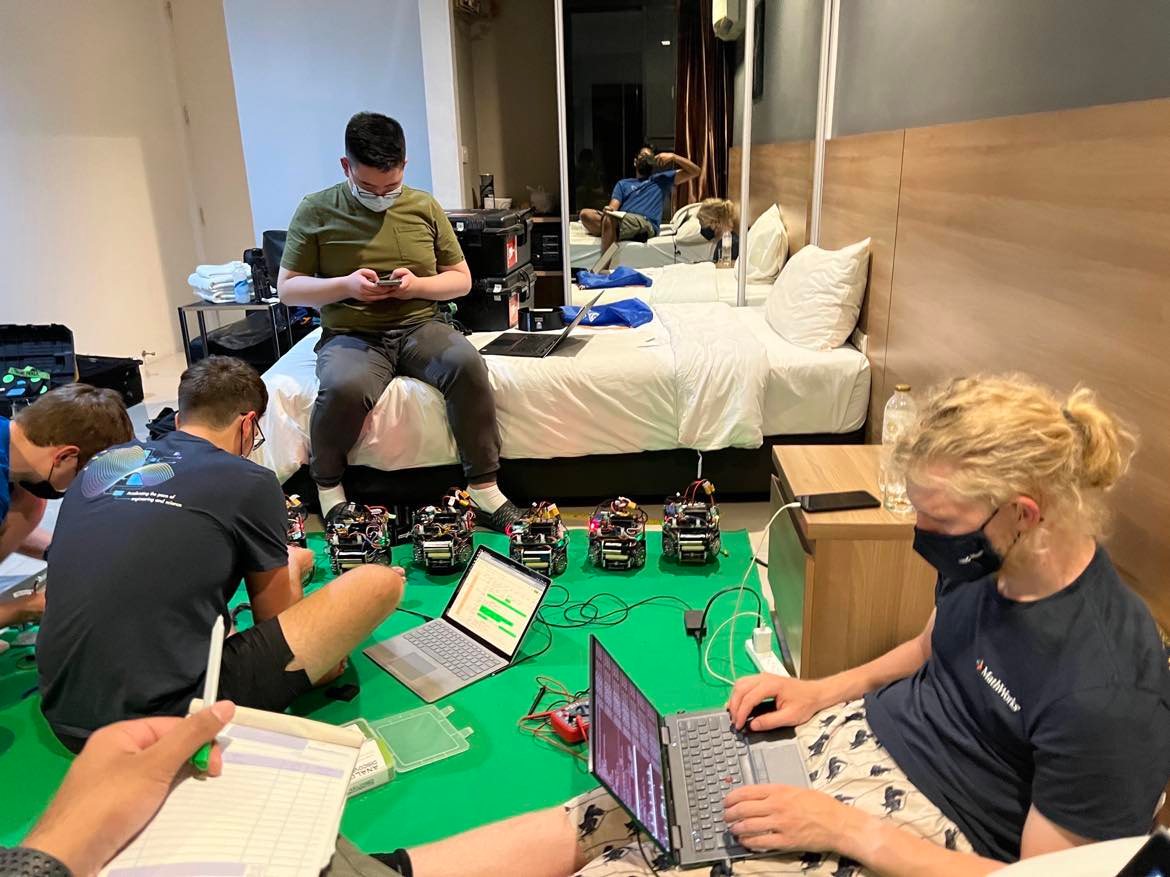
The critical part of testing was during the competition. Undoubtedly, no matter how well the robots are working in the workspace as soon as you bring them to competition new issues will arrive. That to me was the most fun part of compeition. The late nights learning the software workflows to connect to and debug the robots, probing various testpoints on the board while trying to replicate operations that caused failure, coming up with hacky fixes to just get the robots working good enough for competition. These were the dirty, fast fixes that required the most wholistic version of engineering that I found prepared me the most for being an actual engineer.